- 非IC关键词
深圳市科明隆电子有限公司

- 卖家积分:
 营业执照:已审核经营模式:贸易/代理/分销所在地区:广东 深圳企业网站:
http://www.kml-ic.com
收藏本公司 人气:817119
企业档案
- 相关证件:

- 会员类型:
- 会员年限:12年
- 阿库IM:
- 地址:深圳市中航路新亚洲电子城二期N4C738室
- E-mail:1361104728@qq.com
相关产品
产品信息
Features
• Open NAND Flash Interface (ONFI) 1.0-compliant
• Single-level cell (SLC) technology
• Organization
– Page size:
• x8: 2,112 bytes (2,048 + 64 bytes)
• x16: 1,056 words (1,024 + 32 words)
– Block size: 64 pages (128K + 4K bytes)
– Device size: 2Gb: 2,048 blocks
• READ performance
– Random READ: 25μs
– Sequential READ: 25ns (3.3V)
– Sequential READ: 35ns (1.8V)
• WRITE performance
– PROGRAM PAGE: 220μs (TYP, 3.3V)
– PROGRAM PAGE: 300μs (TYP, 1.8V)
– BLOCK ERASE: 500μs (TYP)
• Data retention: 10 years
• Endurance: 100,000 PROGRAM/ERASE cycles
• First block (block address 00h) guaranteed to be
valid with ECC when shipped from factory1
• Industry-standard basic NAND Flash command set
• Advanced command set:
– PROGRAM PAGE CACHE MODE
– PAGE READ CACHE MODE
– One-time programmable (OTP) commands
– BLOCK LOCK (1.8V only)
– PROGRAMMABLE DRIVE STRENGTH
– READ UNIQUE ID
• Operation status byte provides a software method of
detecting:
– Operation completion
– Pass/fail condition
– Write-protect status
• Ready/busy# (R/B#) signal provides a hardware
method of detecting operation completion
• WP# signal: write protect entire device
• RESET required as first command after power-up
• INTERNAL DATA MOVE operations supported
• Alternate method of device initialization
(Nand_Init) after power up4 (Contact Factory)
Figure 1: 63-Ball VFBGA
1. See “Error Management” on page 61.
2. For part numbering and markings, see
Figure 2 on page 2 and Figure 3 on page 3.
3. CPL = center parting line
4. Available only in 1.8V VFBGA package.
Options
• Density2: 2Gb (single die)
• Device width: x8, x16
• Configuration:
# of die # of CE# # of R/B# I/O
1 1 1 Common
• VCC: 2.7–3.6V
• VCC: 1.65–1.95V
• Package
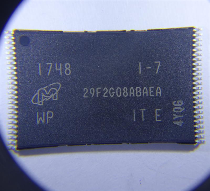
– 48-pin TSOP type I CPL3 (lead-free plating, 3.3V
only)
– 63-ball VFBGA (lead-free, 1.8V only)
• Operating temperature:
– Commercial (0°C to +70°C)
– Extended (–40°C to +85°C)


 询价
询价
